Solar module with potting-free access area in junction box
A photovoltaic module whose junction/connection box contains a potting compound that partially surrounds a bypass device (for example a bypass diode) but deliberately leaves at least one potting-free connection area. Installers or repair technicians can access that potting-free area to add or replace a supplementary bypass component or other electronic component without removing all potting. The connection box contains contact elements that route between the buried bypass device and the exposed connection area.
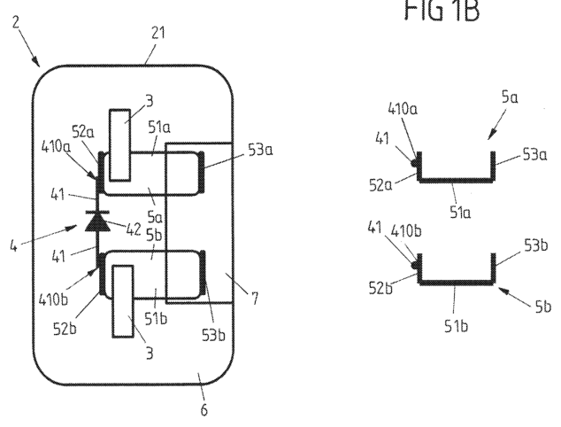
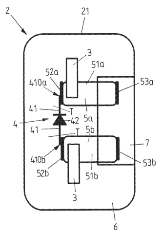
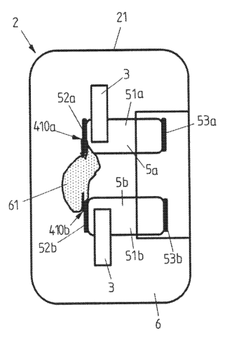
(57) What the patent covered
This write-up was generated by AI from the patent's text and may contain mistakes, so check it against the original patent before relying on it.
The main independent claim covered a solar module having: at least one solar cell; at least two connection elements for electrical connection; a bypass component inside a connection box filled at least partially with potting material; at least one connection area in the connection box that is free of potting material and through which a supplementary bypass component or other electronic component can be connected to the connection elements; and at least two contact elements each with two spaced contact portions, one portion connected to the bypass component and a connection element and the other portion arranged in the potting-free connection area.
Distinguishing feature: Providing a dedicated potting-free connection area in a potted junction box that hosts contact portions routed to a buried bypass device so external components can be added or replaced without complete de-potting.
Novelty 3/5. Bypass diodes in potted junction boxes and potting for protection were already common; the novelty is the deliberate potting-free access area and routed contact portions to permit repair or retrofit.
Manufacturing
Mold or assemble a plastic connection box; place contact elements and the bypass component in position; partially fill the box with potting compound leaving a predefined cavity or recess as the potting-free connection area; cure potting; assemble box onto module backsheet and interconnect with cell cross connectors (soldering or welded tabs).
Materials: Epoxy or polyurethane potting compound, Plastic connection box (likely ABS or polycarbonate), Metal contact elements (tinned copper or brass), Bypass component (silicon diode packaged or discrete semiconductor).
Manufacturability 4/5. Requires standard plastic molding and potting operations plus placement of stamped/wire contact elements and the bypass device; moderate part count and routine assembly processes.
Market demand
No demand check has been run for this patent. Likely search terms: potted solar junction box with access, solar module bypass diode replacement, PV junction box repair area. The links in the sidebar open these searches.
Buyers: PV installers, maintenance technicians, solar module manufacturers doing service.
Before manufacturing
No related continuation or divisional patents in force were found. Design patents, trademarks and unrelated patents may still cover the product.
Practical risks include moisture and corrosion at the intentionally unpotted area, compatibility with UL/IEC PV junction-box certifications, and variability in potting process control; specification details on dimensions and sealing are limited in the patent text.
About 1.5% of lapsed patents are later revived by their owners. This page is a research lead, not legal advice. Obtain a freedom-to-operate opinion before manufacturing.